As a recap, three evidence packages for Device 001 have been released. Evidence Package 1 consisted of raw 2D CT scans of a de-cased, populated PCB that were converted to PNG images. Evidence Package 2 consisted of a high-level hardware Bill of Materials (BOM) for the major integrated circuits and passive components. Evidence Package 3 consisted of high-resolution CT scans of a de-populated PCB.
While this was a fairly simple two-layer circuit board that likely did not require high-resolution scans to understand the device’s functionality, we wanted to familiarize participants with the process we normally employ when analyzing these types of devices. Each of these stages typically results in a level of both human and automated analysis.
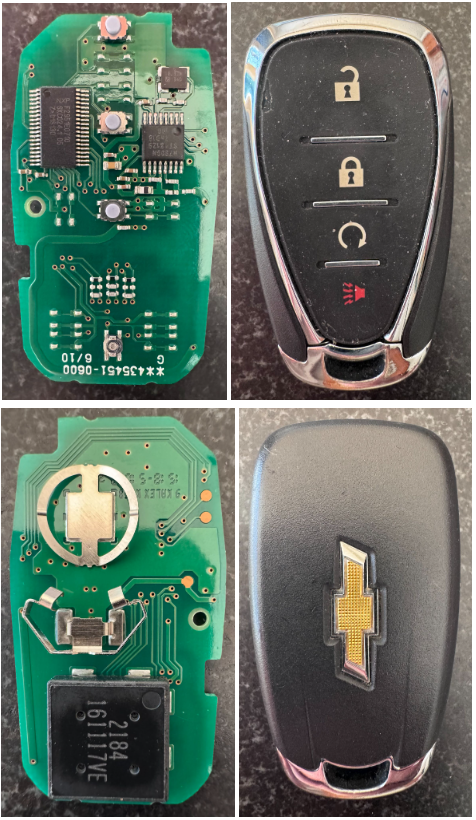
The initial de-casing of the device circuit boards and subsequent photographic imaging drives our hardware BOM analysis, which relies on both our internal component image database and open-source research. In the case of Device 001, this process was relatively straightforward, as all of the components were visible and we did not have to remove any heat sinks or shielding to gain access to the component package labeling.
However, we did encounter another scenario that is common when analyzing new devices in our lab: identifying and matching a component that was not already present in our database. The oscillator was a familiar-looking package size and shape, which was confirmed when we probed the component with an oscilloscope and observed its output. However, the Nihon Dempa Kogyo (NDK) manufacturer logo was not one we were already tracking.
This led us to search through electrical component distributors and datasheets to identify the logo and match it to the manufacturer. While not particularly difficult, this task still required approximately an hour of analyst time.
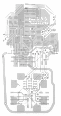
The first 2D scans for this device resulted in a fairly quick understanding of the board. They also provide an excellent way to archive the ground truth of the board before we move into more destructive techniques during subsequent stages of analysis.
In the case of Device 001, the components and board construction are relatively straightforward and much more simplistic than what we normally work on. For more complex devices, or devices for which we only have a single sample, we would typically have an additional stage prior to scanning to allow time for memory offloading or the removal of sensitive components. In this case, however, we proceeded directly to scanning.
The scans confirmed that this was only a two-layer board, demonstrating that there were no hidden nets or blind vias that would complicate tracing electrical paths between components. Additionally, all of the Surface Mount Device (SMD) packages were outline-style packages, where the leads are visible around the perimeter of the device rather than hidden underneath it. This allows us to quickly perform continuity testing on pinouts and reverse engineer the netlist while all components remain in place.
That said, these initial 2D scans are a standard part of our overall process for every device. We always want to document the device as received and establish a baseline for future analysis. This documentation also helps us identify anomalies later, whether on this specific device or across multiple instances of the same device.
The issue with the initial 2D scans of the populated boards is that they contain a lot of “shadows” that are sometimes very difficult, if not impossible, to see through. In other words, dense components on the board block us from seeing what is behind them.
As we saw on this device, we ended up depopulating the board, which is indeed destructive, but gave us a clear, unobstructed view of the PCB in the subsequent scan. These scans allow us to come back to our tools to highlight footprints, identify nets, and ultimately recover the netlist and schematic when paired with the BOM analysis.
Evidence Package 4 (Reveal)