
Last week, we posted Evidence Package 2 for Device 001, which consisted of the high-level Bill of Materials. Almost immediately, we received multiple correct guesses regarding the origins of Device 001. One of the integrated circuits is so specialized that it is fairly indicative of the device’s logical function. While we have a couple of correct guesses, we are going to continue the 001 series so people can become more familiar with the process, tools, and artifacts.
This week, we will take a closer look at the board itself. While this is a fairly small board (handheld size), it is not very densely populated. We began by depopulating the board in order to obtain very clear CT scans. While it would be possible to recover the board design by tracing the pads with an ohmmeter, we decided to leverage the tools available to us and generate full, clean, shadowless scans. The ideal end artifact is a complete board layout and, when combined with the Bill of Materials, an eventual reconstruction of the schematic.
Evidence Package 3 (Board Layout)
Artifacts
The CT scans from Evidence Package 1 contained all of the board components at the time of the scan. While this method is obviously less destructive to the device, it brings forward some challenges. When the ICs are on the board (in more complex designs), ball grid array-style surface packaging makes manual trace recovery difficult, as we cannot put probes onto simple perimeter pinouts like those on this board.
However, when we keep the components on the board and do a CT scan, there are a number of shadows created by the components that obscure the board details. With the components removed, a much cleaner image can be obtained, but we do lose the ability to Ohm out a trace in some cases where a passive component, like a resistor, is no longer present to complete the trace path.
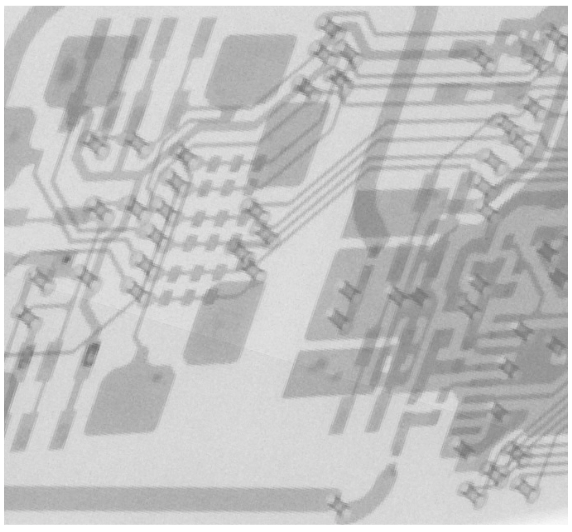
That is why we typically conduct both scans and perform manual analysis at both stages of our process. Below, you will see the CT images from Side 1 and Side 2 of Device 001.
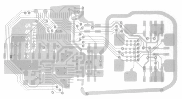
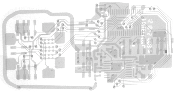
We say Side 1 and Side 2, but clearly that doesn’t make much sense when you are actually looking at Side 1 and Side 2 simultaneously in a single image, as we can effectively see through the board. When we smash a three-dimensional image down to two dimensions, there are a couple of nuances that need to be accounted for.
During PCB development, developers tend to use colors to track the various board layers. In this grayscale 2D version, however, the layer information is not present when coming directly off the CT scanner. As an example, look at the trace in the lower left of the second board view. At first glance, you may wonder what elementary school drawing device was used to draw the trace, as there appears to be a very odd overlap at the vias.
Then, remembering that those are vias, and that two of those traces are on one side of the board while the other trace is on the opposite side, it makes much more sense why this is not a continuous flowing line.
The nice part about our imaging software is that we can pull three-dimensional images from a scan. This is extremely helpful when trying to recover trace paths from a multi-layer squashed view. If we can start at the pads under an IC, we can walk the traces one edge at a time as they meander through the layers to get to their destination.
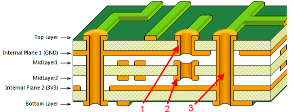
In schematic view, electronic designs are fairly straightforward. Schematics do not have to take physical dimensions into account. In board design, however, space is limited, and when there are a lot of dense ICs in a small physical package, designers need to use layers in order to get traces from point A to point B without crossing other traces.
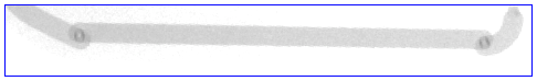
In this isometric view below, you can see the actual depth of the board and even the full plating of the vias themselves. This is very helpful when going through the process of marking up the image and recovering a board layout.
In this case, one thing that is apparent is that we are looking at a 2-layer board, and we can clearly see traces on the top and bottom layers with only through vias. This is where CT scanning really shines.
Future devices we post will have more than two layers, and finding these buried vias on 6-layer boards does aid in the understanding of a board layout.
We will leave you with the two views above if you want to start trying to reconstruct the schematic using the BOM knowledge. If you need additional views or the original files, feel free to reach out.